
Samsung Unveils Next-Gen HBM4E Memory and Deepens NVIDIA Partnership at GTC 2026
Samsung Electronics took center stage at NVIDIA’s GTC 2026 conference in San Jose this week, unveiling its most advanced memory technologies yet and reaffirming a sweeping strategic partnership with NVIDIA that spans chip design, manufacturing, and AI infrastructure.

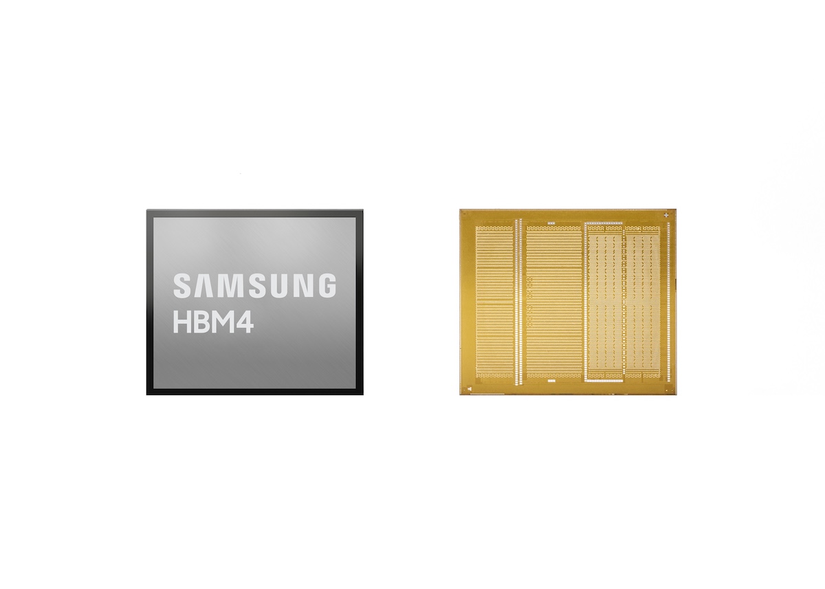
The headline announcement was Samsung’s sixth-generation High Bandwidth Memory chip, HBM4, now in mass production and purpose-built for NVIDIA’s upcoming Vera Rubin platform. The chip delivers processing speeds of 11.7 gigabits per second, nearly 50 percent above the industry standard of 8Gbps, with the potential to reach 13Gbps. But Samsung didn’t stop there. The company offered the industry’s first public look at its successor, HBM4E, which pushes performance even further to 16Gbps per pin and 4.0 terabytes per second of bandwidth.
Both chips are built on Samsung’s most advanced 10-nanometer-class DRAM process, which the company says has enabled stable manufacturing yields alongside the performance gains.
Also on display was Samsung’s hybrid copper bonding (HCB) technology, a packaging innovation that allows future HBM chips to stack 16 or more layers while cutting heat resistance by over 20 percent compared to current methods, a critical advancement as AI chips continue to run hotter and denser.

A dedicated “NVIDIA Gallery” within Samsung’s booth underscored just how closely the two companies are now working together. On show were Samsung’s SOCAMM2, a low-power, high-bandwidth server memory module already in mass production, and the PM1763 SSD, based on the blazing-fast PCIe 6.0 interface, demonstrated running on servers using NVIDIA’s SCADA programming model.
The collaboration extends well beyond hardware. Samsung revealed plans to deploy NVIDIA accelerated computing within its own AI Factory operations, including digital twin manufacturing powered by NVIDIA Omniverse. The initiative positions Samsung’s chip manufacturing infrastructure — covering memory, logic, foundry, and advanced packaging,as one of the most comprehensive in the world.

Yong Ho Song, Samsung’s Executive Vice President and Head of AI Center, addressed the partnership in a speaker session on March 17, detailing how agentic AI and digital twins are reshaping semiconductor manufacturing from design all the way through to production.
Samsung also turned attention to the edge, showcasing LPDDR5X and LPDDR6 memory designed for smartphones, tablets, and wearables. LPDDR5X reaches 25Gbps per pin while reducing power consumption by up to 15 percent. Its successor, LPDDR6, scales bandwidth to between 30 and 35Gbps per pin, introducing adaptive voltage scaling and dynamic refresh control, features aimed squarely at the growing demands of on-device AI applications.
Together, the announcements paint a picture of a company positioning itself as the singular end-to-end semiconductor partner for the AI age, from the massive GPU clusters powering cloud AI, down to the chip inside a consumer’s wristwatch.
Mark your calendars! The GreenShift Sustainability Forum is back in Nairobi this August. Join innovators, policymakers & sustainability leaders for a breakfast forum as we explore sustainable solutions shaping the continent’s future. Limited slots – Get your early bird tickets now – here. Email info@techtrendsmedia.co.ke for partnership requests.
Go to TECHTRENDSKE.co.ke for more tech and business news from the African continent and across the world.
Follow us on WhatsApp, Telegram, Twitter, and Facebook, or subscribe to our weekly newsletter to ensure you don’t miss out on any future updates. Send tips to editorial@techtrendsmedia.co.ke